Advanced Logic Technology Solutions
Advanced logic technology development (FinFET and beyond) requires the exploration of new materials and transistor structures to achieve optimal performance, power, area, cost and manufacturing yield. A major challenge in advanced technology development is to identify the best architecture as early as possible manner while covering all the possible device and process technology options.
Our suite of high-fidelity process, device and lithography simulators enable evaluation of device and process options well before any wafer is available. The design connectivity tools, generate TCAD-based compact model for devices and parasitic RC netlists for circuit blocks, and further enable analyses on performance, power, area, cost and manufacturing yield metrics.

In the continuous development of advanced logic technology, DTCO (Device-Technology Co-Optimization) plays a crucial role. Especially with the emergence of FinFET and higher-level technologies, the exploration of new materials and transistor structures has become increasingly urgent in seeking the optimal balance between performance, power consumption, area, cost, and manufacturing yield. However, in the process of advancing these advanced technologies, a significant challenge lies in how to determine the optimal architecture as early as possible, while covering all possible device and process technology options comprehensively.
To address this challenge, we have introduced a high-fidelity process, device, and lithography simulator suite. This innovative tool suite enables precise evaluation of various options for devices and processes before any wafers are actually available. This not only helps us identify potential issues and bottlenecks early on but also allows targeted optimization at the design stage, significantly enhancing the performance of the final product.
Furthermore, we also use design connectivity tools to generate compact models based on TCAD (Technology Computer Aided Design). These models accurately reflect the parasitic RC network list of devices and circuit blocks, providing in-depth analysis for performance, power consumption, area, cost, and manufacturing yield. Through this approach, we can promptly identify and correct potential defects in the design process, ensuring that all indicators of the final product meet the expected goals.
In summary, our high-fidelity process, device, and lithography simulator suite, as well as the TCAD-based compact model generation tool, provide strong support for DTCO in advanced logic technology. They not only help us achieve co-optimization of devices and technologies but also drive continuous progress and development in the entire field of advanced logic technology.
Back-Side Power-Delivery Network (BSPDN) – A Design–Technology Co-Optimization (DTCO) Example
Background and Objectives
In advanced logic technologies, FinFET has become the predominant transistor architecture. In addition to the transistor, the metal-based power-delivery network (PDN) is a crucial factor influencing circuit performance. As technology nodes shrink, traditional front-side power-delivery networks (FSPDNs) encounter significant challenges, including increased IR drop from higher wire resistance and diminished routing efficiency due to congested front-side metal layers. Back-side power-delivery networks (BSPDNs) have emerged as a viable solution by relocating power rails to the back side of the wafer, thus alleviating these challenges.
There are various BSPDN technology options, each offering multiple process choices and parameters. The Design Technology Co-Optimization (DTCO) methodology is essential for selecting the optimal technology path and refining process options and parameters. By employing device-process co-optimization, engineers attain an optimal balance of performance, power, area, and cost (PPAC).
Solution
The Mozz Process is employed to produce a conventional front-side-powered FinFET structure (refer to the lower left figure), and a FinFET featuring back-side contacts (BSC) (refer to the lower right figure).
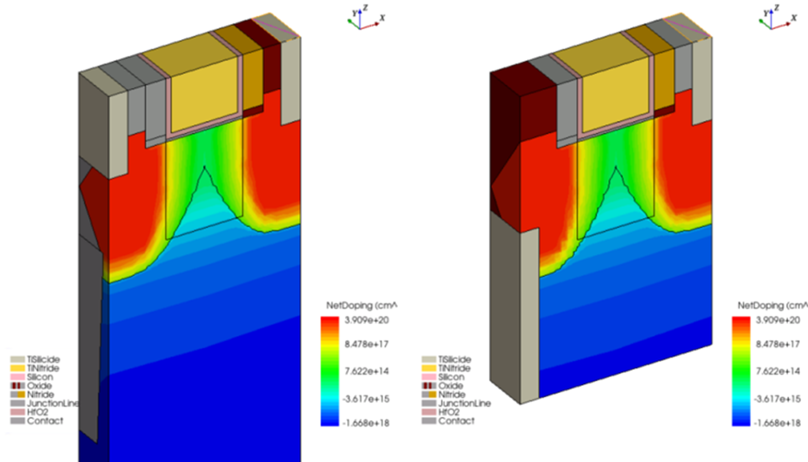
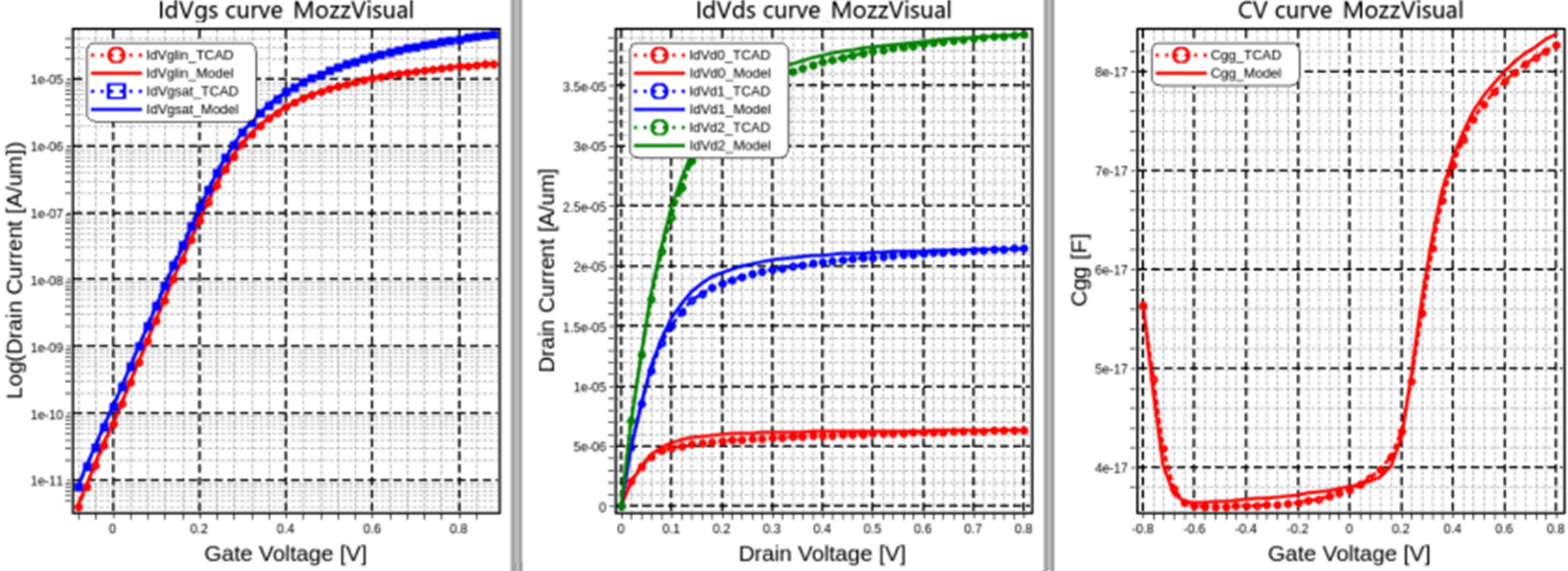
The Mozz Device simulates the current-voltage (I–V) and capacitance-voltage (C–V) characteristics of both structures, while the Mozz Extract generates the corresponding compact models.
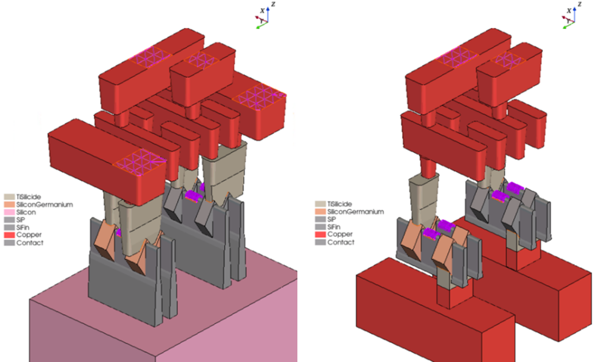
The Mozz ProcEmu (also known as Mozz Structure) constructs a standard-cell inverter featuring a front-side power distribution network (PDN) as shown in the lower left figure, and an equivalent standard-cell inverter incorporating a back-side PDN as illustrated in the lower right figure. The Mozz RCEx tool extracts the parasitic resistance-capacitance (R-C) netlist for each cell.
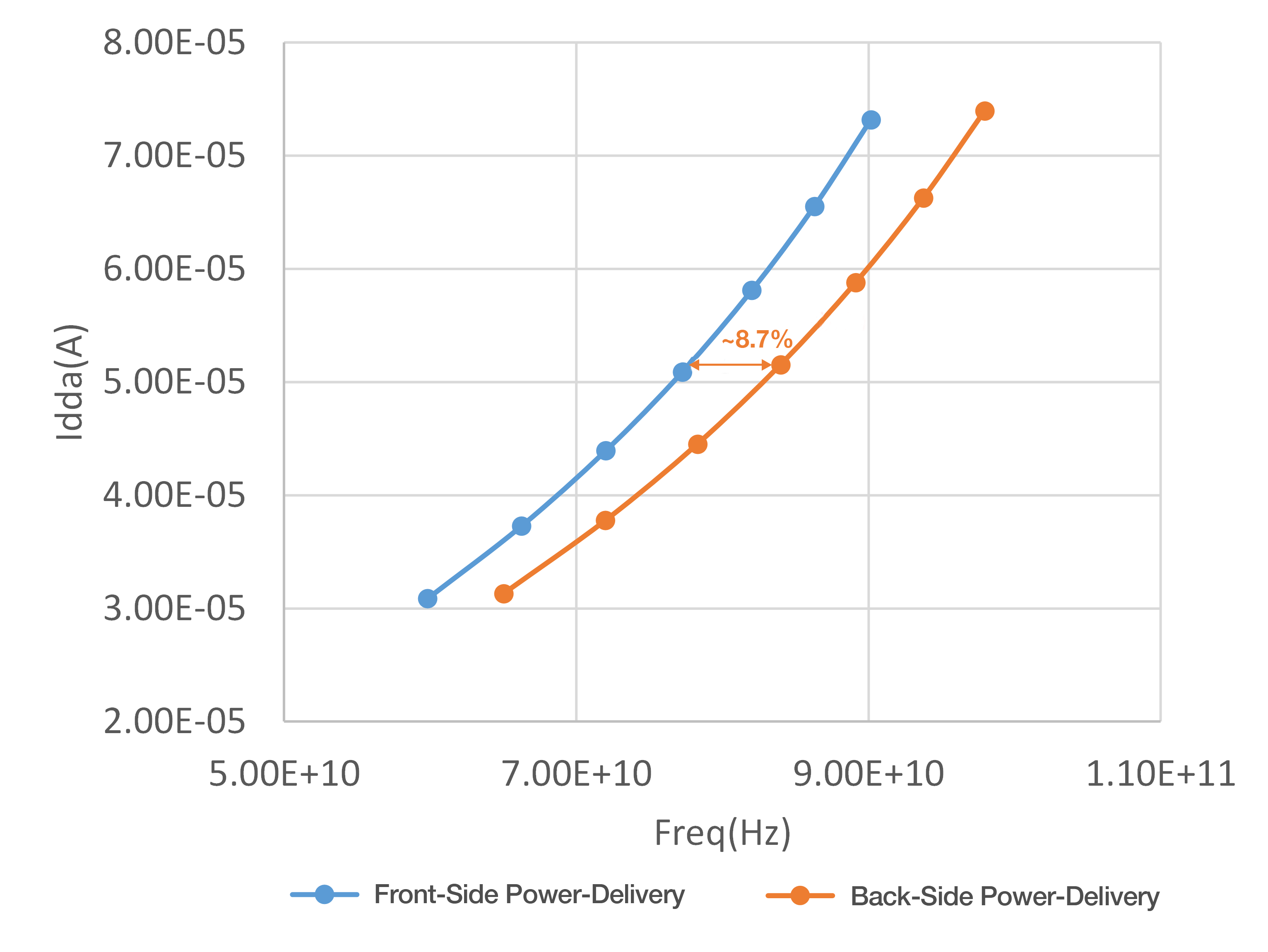
SPICE-level circuit simulations were conducted to compare the performance of ring oscillators (ROs). The results indicate a significant advantage in speed and power efficiency for the back-side power-delivery ring oscillator.
Case Summary
The application of the Design Technology Co-Optimization (DTCO) flow, which integrates FinFET structural optimization with back-side process integration, enables efficient deployment of BSPDN. Accurate modeling and optimization improve device performance and power efficiency while simultaneously reducing costs, thereby strongly supporting the ongoing advancement of advanced logic technologies.
