Y-CHIP Design Platform
Back Ground
In the period of instore new process, yield will improve from 0% to`100%. Test chip can help to verify the key block of process, find and deal with the issue earlier. Y-CHIP solution can meet the requirement of test and verification.
Design Method
Y-CHIP design should obey the rule:
- Cover diversified rule and layout: integrate different design rule and layout for cross check, then select better method.
- Diversified OPC scheme: cover different OPC scheme, select the best by testing.
- Design test platform based on fundamental circuit: such as standard cell, IO, SRAM, importance IP and so on.
- Cover all standard cell and IO: cover all standard cell and IO, support mini-PAD to test by nano-probe.
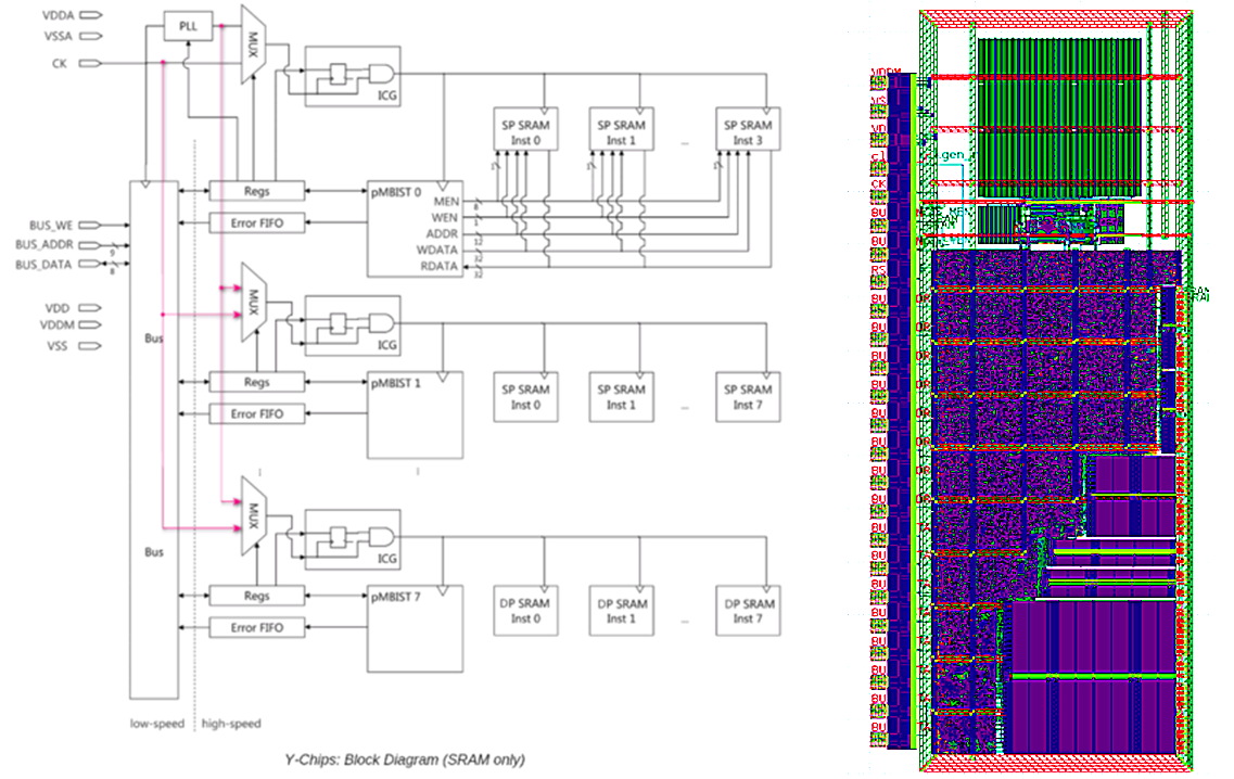
- Design SRAM array to test function and performance: include all SRAM cell type and array, enough capacity for yield test. Design BIST circuit, and design instance based on library data for performance test.
Example: Y-CHIP test platform in one process
Y-CHIP for advanced process testing in instore period, has the characteristic:
Characteristic:
- BIST design, lower dependency of ATE
- Integrated PLL, support high performance test
- Testable SRAM ARRAY to test the yield of SRAM cell
- More SRAM instance to cover different array capacitance
- Build in all standard cell and the test circuit
- Include digital block design based on standard cell
- 24 PAD for function and performance test
Advantage
- Integrated function, performance and yield test of the new process
- Support parallel test to accelerate the yield improving
- Connect to ATE easily, and industrialization easily
