Low Cost Design Solution
Design Method
Usually, digital circuit design use standard cell and SRAM IP supported by FAB. But the general IP is not area optimal. In some case, use customized standard cell and SRAM IP, will decrease the circuit area, and make low cost.
Standard Cell Improvement
- Traditional: standard cell supported by FAB is balanced with speed, power and routing, apply most design, but not area optimal.
- Optimization: in some typical case, customized standard cell can match the timing and routing, and decrease the area
- Effect: based on different process and requirement, the area of standard cell library can reduce about 30%.
- Application: customized standard cell will be slower and has smaller routing channel,should use in low frequency and sparse routing design.
SRAM IP Replace Solution
- SRAM issue: SRAM cell designed with high density rule, but periphery circuit for reading and writing obey standard DRC rule. So small capacitance SRAM IP area may larger than DFF array.
- Use DFF array: If capacitance < 8K bit, replacing SRAM IP by DFF array will make smaller area. And replace conveniently by PIN-to-PIN replacement design.
- **More optimization:using Latch Array to replace DFF array, will decrease the area more. And normal DFF array can be replaced by latch array to decrease area more.
- Area gain: in some case, latch array area will shrink about 50% compared with DFF array.
Example: low cost design in internal project
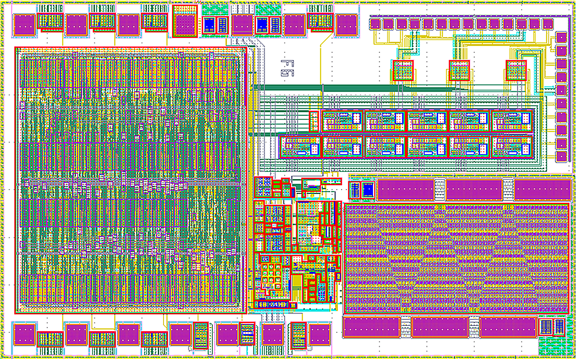
- Customized Standard Cell: Use customized Standard Cell in one project, the area shrink is about 30%.
- Replacing DFF array: replacing DFF array by Latch array in some blocks, the area shrink is about 55%.
- No SRAM IP: use DFF/Latch array, no SRAM IP in design.
