FinFET Single Event Effects
Methodology
For an SOC or FPGA manufactured with 16nm/7nm finFET process, single event latch-up (SEL) might happen to the IO part, or single event upset (SEU) might happen to the core part.
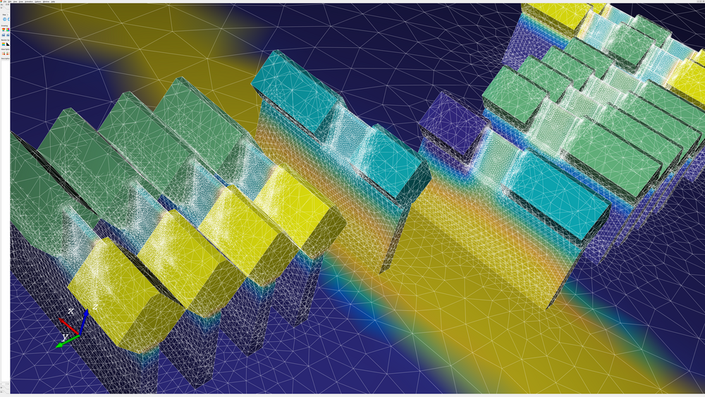
Based on 3D TCAD process simulation, (or one may prefer another way 3D structure builded directly), the structure and doping profiles of finFET devices can be established. Combined with energetic particle simulation, TCAD device simulations will give the device or circuit response to the striking particle.
Typical applications:
- Detailed simulation of the SEL/SEU phenomena, reveals the laws of SEL/SEU.
- Find the sensitive parts of SEL/SEU
- Find the exact mechanism of SEL/SEU
- Find the conditions (voltages, temperature, etc) of SEL/SEU
- Fine multi cell upsets
- Determine the SEU cross-section
- Check or verify hardening designs
Example
Figure below gives a SEU Map of a configuration SRAM cell manufactured with 16nm finFET process. From it the sensitive part of the cell can be seen clearly.
Hardening
Typical SEL hardening methods include separation, guard rings, or contacts, which means that there will be a trade-off between chip area and hardening effect.
Employing this fully physical simulation, one can estimate the hardening effects without taping-out or heavy-ion tests. Thus find out the best hardening solutions.
